The Intel Haswell-E CPU Review: Core i7-5960X, i7-5930K and i7-5820K Tested
by Ian Cutress on August 29, 2014 12:00 PM EST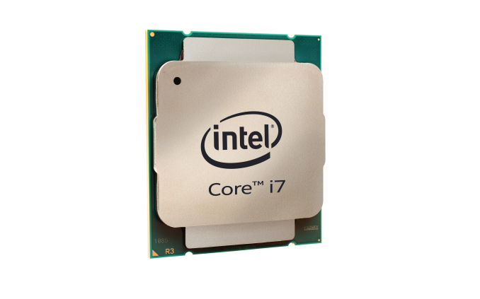
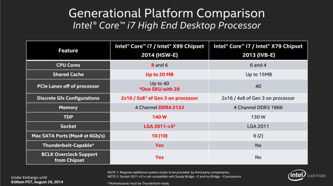
Today marks the release of Intel’s latest update to its Extreme processor line with a trio of Haswell-E models including Intel’s first consumer socketed 8-core product. This is the update from Ivy Bridge-E, which includes an IPC increase, a new X99 chipset, the first consumer platform with DDR4 memory, and a new CPU socket that is not backwards compatible. We managed to get all three CPUs ahead of launch to test.
August 29th, The Haswell-E Launch
As part of PAX Prime today, three major launches are occurring:
- New line of Haswell-E i7 CPUs
- New line of X99 motherboards using the new LGA2011-3 socket
- An upgrade from DDR3 to DDR4 memory, using the new 288-pin slots
Each of these launches is an upgrade over the previous enthusiast models in the market. The Haswell-E processors will support up to 8 cores on i7, the X99 motherboards have increased connectivity and focus on newer storage methods, and the DDR4 memory supports higher frequency memory at lower voltages than DDR3.
Our coverage will be split to cover all three major launches. This article is talking about the Haswell-E CPUs, we will have another article discussing the new X99 chipset and motherboards, with a third about the new DDR4 memory. There is a small amount of overlap in the data between the three, but check out our other articles this week to find out more.
The New CPUs
Getting straight to the heart of the matter, Intel is keeping the enthusiast extreme range simple by only releasing three models, similar to the initial Sandy Bridge-E and Ivy Bridge-E launches.
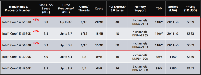
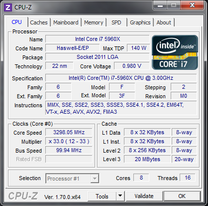
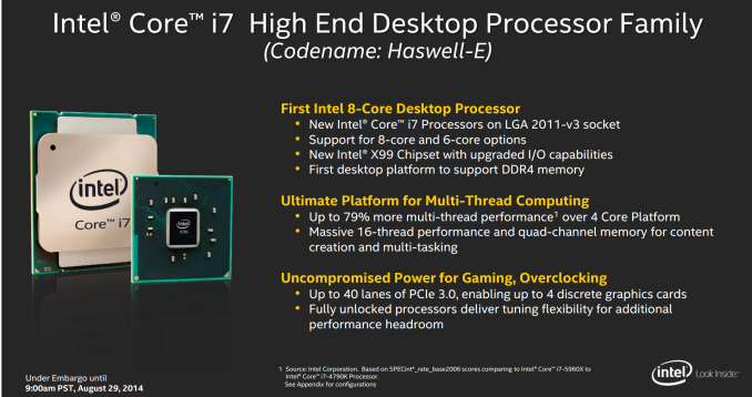
The top of the line will be the 8-core i7-5960X with HyperThreading, using a 3.0 GHz base frequency and 40 PCIe 3.0 lanes for $999 for 1000 units. This pricing is in line with previous extreme edition processor launches, but the base frequency is quite low. This is due to the TDP limitation: sticking two extra cores produces extra energy lost as heat, and in order to get the TDP down the base clock has to be reduced over the six-core models. This is a common trend we see in the Xeon range, and as a result it might affect the feel of day-to-day performance.
The mid-range i7-5930K model mimics the older i7-4960X from Ivy Bridge-E by having six cores and 40 PCIe 3.0 lanes, however it does differ in the frequencies (the 5930K is slower) and the memory (5930K supports DDR4-2133). Pricing for this model is aimed to be highly competitive at just under the $600 mark.
The entry level model is a slightly slower i7-5820K, also featuring six cores and DDR4-2133 support. The main difference here is that it only has 28 PCIe 3.0 lanes. When I first read this, I was relatively shocked, but if you consider it from a point of segmentation in the product stack, it makes sense. For example:
For Ivy Bridge-E and Sandy Bridge-E, the i7-4820K and i7-3820 CPUs both had four cores, separating it from the other six cores in their series. For Nehalem, the quad core i7-920 was a super low clocked version compared to the quad core i7-965 and hex-core i7-980X which was released later. In these circumstances, the options for the lower $400 part were either fewer cores or lower frequency. Intel has decided to make the lower cost Haswell-E processor with fewer PCIe 3.0 lanes, but this is an even better scenario for most consumers:
Having 28 PCIe 3.0 lanes means dual GPU setups are at PCIe 3.0 x16/x8 (rather than x16/x16), and tri-GPU setups are at x8/x8/x8 (rather than x16/x16/x8). Very few PC games lose out due to having PCIe 3.0 x8 over PCIe 3.0 x16, meaning that performance should be almost identical. On paper, there should be a smaller performance difference with this setup than if the frequency had been reduced, or the fact that people would complain if there were fewer cores. Having six cores puts it above the i7-4790K in terms of market position and pricing, and the overall loss is that an i7-5820K user cannot use 4-way SLI, which is a very small minority to begin with.
The only downside to all the 28 PCIe 3.0 lanes is that there is no physical way to improve the PCIe lane situation. If the frequency was low, the user could overclock. If there were fewer cores, overclocking would also help mitigate that. Despite this, on paper it looks like that performance difference should be minimal.
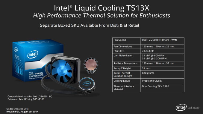
The raise in TDP from 130W to 140W puts extra strain on user cooling. Intel still recommends its TS13X liquid cooling solution as a bare minimum – this is the same cooling solution Intel suggested for Ivy Bridge-E. Users wanting to overclock might expect another 150W pushing the i7-5960X up to 4.3 GHz (see our overclocking results later in the review), suggesting that an aftermarket thicker/longer radiator liquid cooler might be in order.
The CPU
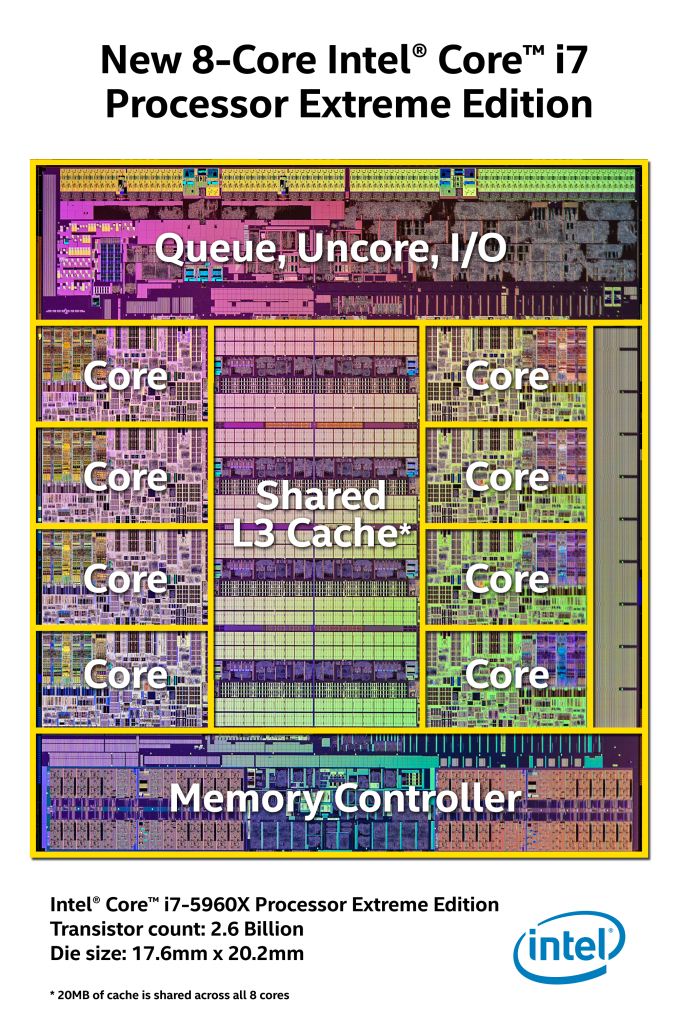
The base silicon for the three mainstream Haswell-E processors is of a similar construction to the previous generation, with a dedicated L3 cache in the middle and the processors around the outside connected by a ring:
All eight cores in the silicon will have access to the cache for the top of the line Core i7-5960X. For the six core models, the i7-5930K and the i7-5820K, one pair of cores is disabled; the pair which is disabled is not always constant, but will always be a left-to-right pair from the four rows as shown in the image. Unlike the Xeon range where sometimes the additional cache from disabled cores is still available, the L3 cache for these two cores will be disabled also.
Intel was quite happy to share the dimensions of the die and the transistor counts, which allows us to update this table with the new information:
| CPU Specification Comparison | |||||||||
| CPU | Manufacturing Process | Cores | GPU | Transistor Count (Schematic) | Die Size | ||||
|
Intel Haswell-E 8C |
22nm | 8 | N/A | 2.6B | 356mm2 | ||||
|
Intel Haswell GT2 4C |
22nm | 4 | GT2 | 1.4B | 177mm2 | ||||
|
Intel Haswell ULT GT3 2C |
22nm | 2 | GT3 | 1.3B | 181mm2 | ||||
|
Intel Ivy Bridge-E 6C |
22nm | 6 | N/A | 1.86B | 257mm2 | ||||
|
Intel Ivy Bridge 4C |
22nm | 4 | GT2 | 1.2B | 160mm2 | ||||
| Intel Sandy Bridge- E 6C | 32nm | 6 | N/A | 2.27B | 435mm2 | ||||
| Intel Sandy Bridge 4C | 32nm | 4 | GT2 | 995M | 216mm2 | ||||
|
Intel Lynnfield 4C |
45nm | 4 | N/A | 774M | 296mm2 | ||||
|
AMD Trinity 4C |
32nm | 4 | 7660D | 1.303B | 246mm2 | ||||
|
AMD Vishera 8C |
32nm | 8 | N/A | 1.2B | 315mm2 | ||||
This shows how moving from a six core Ivy Bridge-E die to an eight core Haswell-E increases the die area from 257 mm2 to 356 mm2 (a 39% increase) and the number of transistors from 1.86 billion to 2.6 billion (a 40% increase). This means that adding 33% more cores actually requires more space and more transistors. Part of the increase as well might be the migration to a DDR4 memory controller.
The span of the extreme processor space historically from Intel has a distinct pattern. The CPUs with the lower cores are often clocked the fastest, but over time the speed of the SKU with the most cores might match the lower core model. Then when the next update arrives with more cores, the frequency is again reduced:
| Intel Extreme Edition Comparison | |||||
|
Nehalem (130W) |
Sandy Bridge-E (130W) |
Ivy Bridge-E (130W) |
Haswell-E (140W) |
||
|
Four Cores |
<3.0 GHz | i7-920 | |||
| 3.2 GHz | i7-965 | ||||
| 3.6 GHz | i7-3820 | ||||
| 3.7 GHz | i7-4820K | ||||
|
Six Cores |
3.2 GHz | i7-3930K | |||
| 3.3 GHz | i7-980X | i7-3960X | i7-5820K | ||
| 3.4 GHz | i7-4930K | ||||
| 3.5 GHz | i7-990X | i7-3970X (150W) | i7-5930K | ||
| 3.6 GHz | i7-4960X | ||||
|
Eight Cores |
3.0 GHz | i7-5960X | |||
When you take the cache sizes into account (click a CPU to see the cache size), it becomes very difficult to do a like-for-like comparison. For example, the i7-990X and the i7-5930K are both six-core, 3.5 GHz base frequency models, but the i7-5930K has 3MB more L3 cache. Similarly with the i7-980X and the i7-3960X.
| Nehalem |
Sandy Bridge-E |
Ivy Bridge-E |
Haswell-E |
The X99 Chipset
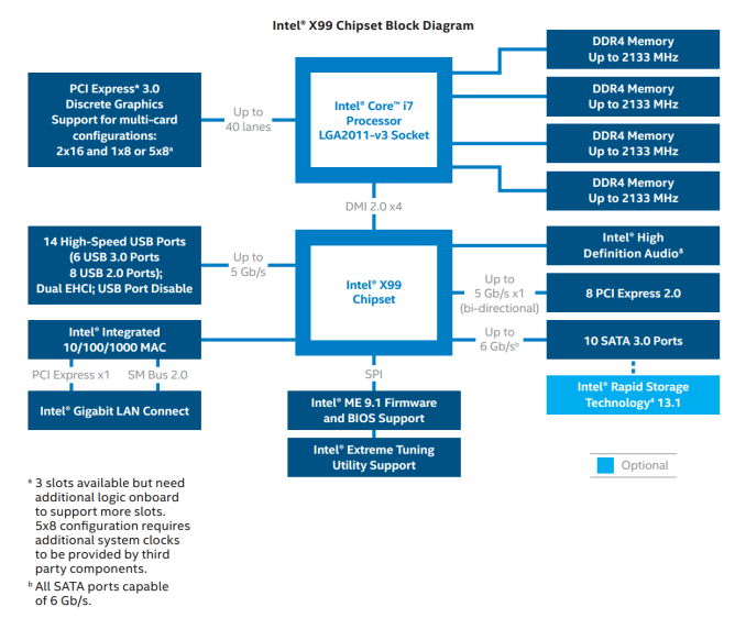
We will go into more detail in our motherboard review piece, but the basic X99 chipset layout from Intel is as follows:
For CPUs with 40 PCIe lanes, the chipset diagram above will allow x16/x16/x8 scenarios or x8/x8/x8/x8/x8 with additional clock generators. For the 28 lane CPU, this becomes x16/x8/x4, which might make some PCIe slots on the motherboard redundant – it is worth checking the manual first which should show each combination. With ASUS motherboards, they have implemented a new onboard button which tells 2x/3x GPU users which slots to go in with LEDs on the motherboard to avoid confusion.
The platform now uses DDR4 memory, which has a base frequency of 2133 MHz. Almost all consumer motherboards will use either one DIMM per channel or two DIMMs per channel, making up to 64GB of memory possible with the latter. Should 16GB UDIMM DDR4 modules come along, it is assumed that with a microcode update, Intel will support these as well.
X99 will also support 10 SATA 6 Gbps ports from the chipset. This is a rather odd addition, because only six of those ports will be RAID capable. Most motherboards will list which ones are specifically for RAID, but this dichotomy makes me believe that the chipset might use a SATA hub on die in order to extend the number of possible ports.
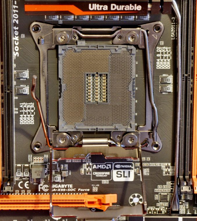
The socket looks roughly the same from X79 to X99, but the main differences include the notches inside the socket, making sure that you cannot misplace the wrong CPU in the wrong socket. The pin layouts are also different, making them incompatible. The socket arms for fixing the CPU in place also change, with X99 arms requiring to be pushed around and out rather than out then in.
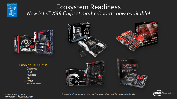
All the main motherboard manufacturers will have models ready on day one. These will be in the micro-ATX and ATX form factors, with most models aiming at the high end for functionality and performance such as the ASUS X79 Deluxe and the ASRock X99 OC Formula. There will be a few models for the cheap side of the market, such as the MSI X99S SLI PLUS and the GIGABYTE X99-UD3.
Prices should range from around $230 to $400+. See our X99 motherboard coverage for a more in-depth look.
DDR4 and JEDEC
All the Haswell CPUs will support DDR4 only, and the new DDR4 design means that the DRAM slots will not be able to take DDR3 due to a different placement of the notch and DDR4 has more pins. DDR4 modules are also a slightly different shape whereby the middle pins of the memory are longer than those on the outside.
For motherboards with single sided latches, this can make it a little trickier to put in because the module might feel in place but both ends need to be firmly in the slot.
The CPUs are listed as supporting DDR4-2133 which in terms of JEDEC timings is 15-15-15. This is similar to when DDR3 first launched, at the nice low (but high at the time) speed of DDR3-1066 7-7-7. While DDR4-2133 CL15 sounds slow, DRAM module manufacturers will be launching models up to DDR4-3200 CL16. This turns the DRAM Performance Index (MHz divided by CAS) from 142 to 200.
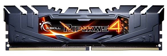
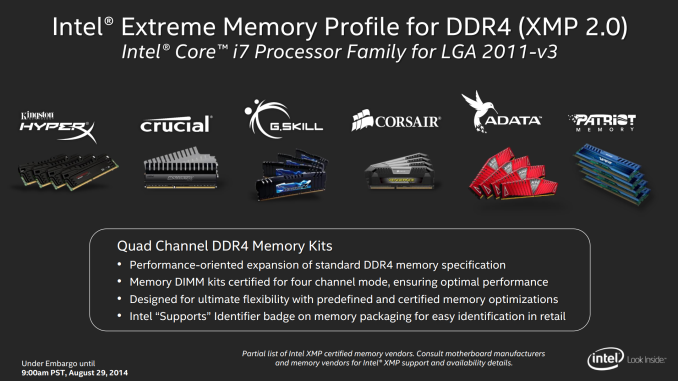
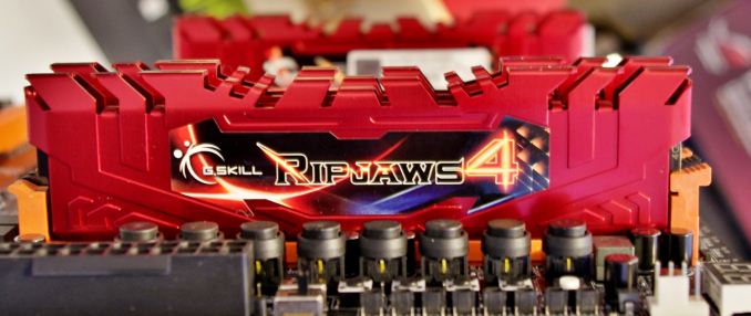
DDR4 is also at a lower voltage than DDR3, with 2133 C15 modules requiring 1.2 volts. Prior to launch, G.Skill, Corsair, Crucial and ADATA all sent out preview images of their modules, with a few even releasing pricing to etailers ahead of time.
Modules should be available from DDR4-2133 to DDR4-3200 at launch, with the higher end of the spectrum being announced by both G.Skill and Corsair. See our DDR4 article later this week for more extensive testing.
Haswell-E and the Battle with Xeons
One of the main issues Intel has with its Extreme platform is the respective enterprise platform based on its high end Xeon processors. In the server world, the customers demand a certain level of consistency for each platform to match up with their upgrade and replacement cycle. As a result, while mainstream Haswell processors were launched in June 2013, it has taken another 14 months for the enthusiast versions to hit the market. This cadence difference between mainstream and extreme silicon is primarily driven by the Xeon market requiring the same platform for two generations. In this case, the Sandy Bridge-E and Ivy Bridge-E platforms, with the LGA2011-0 socket, we held in place for three years before the upgrade to Haswell-E with LGA2011-3. If you are wondering why there is the big difference in release date from Haswell to Haswell-E, there is your answer.
That being said, the consumer range of extreme processors is actually a small market for Intel compared to the Xeons. The market is pushed more out of the prosumer level customers that require performance but at a lower cost, or as a platform for Intel to show how fast it can go at a certain power limitation and then allow extreme overclockers to blow through it as much as possible.
The prosumer market is the important one for the consumer grade silicon. For small businesses that rely on CPU limited throughput, such as video editing, video production, scientific computation and virtualization, having the high performance in a single, low-cost product can produce a significant upgrade in throughput, allowing projects to be completed quicker or with more accuracy. While these prosumer would love the higher powered Xeons, the cost is overly prohibitive, particularly in the long term, or the lack of memory overclock capability has a negative effect.
With this long delay in extreme platform upgrades, it gives Intel the chance to test new functionality out on the mainstream segment. One of the prevailing problems with Ivy Bridge-E is that it relies on the X79 chipset which is showing its age. The new Haswell-E platform and the X99 chipset borrows plenty of cues from Z87 and Z97 in terms of input/output and connectivity support, based on the Xeon customer request of ‘SATA Express looks good, we will have that’.
The drive for lower power is also true, even in high performance systems. For datacenters, the majority of the cost of the facility is typically the energy usage for the systems and the cooling. Thus if a datacenter can use a more energy efficient system, it probably will. So the transition from DDR3 to DDR4 also involves a drop in DRAM voltage from 1.5 volts to 1.2 volts. This does not sound like much for a home system with 4-8 DRAM modules, but in a datacenter with several thousand systems, each using 8-64 sticks of memory, saving a few kW helps bring down the power bill.
This extreme cadence will eventually land Intel with a bit of an issue. If the gap between the mainstream CPU architecture and the performance CPU architecture widens more, then at some point there will be a two-generation difference. This means the server side will have to decide if having fewer faster cores with the highest IPC on the market is better than 2-3 year old slower processors. This would also mean a dichotomy based on whatever features are added. This would suggest that at some point, Intel may have to cut out an entire platform of processors but still maintain the two-generation platform consistency that the server market requires.
Competition and Market
Perhaps unsurprising Intel’s main competition is from itself on the consumer CPU side. As in the table above, the 5960X now leads the new charge on 8-core processors with the 6-core i7-5820K sitting at the back with a reduced lane count but also with a reduced price. Doing a direct comparison based solely on frequency and core count we can see that the i7-3960X matches the i7-5820K, showing how the platform evolves (as well as a position of the price point) over time. This bodes well, perhaps suggesting that Skylake-E’s lowest processor will be a similarly specified Haswell-E i7-5960X but with a higher IPC, should the trend continue.
Intel’s nearest challenger for consumer CPUs from outside is still the FX-9590 which we reviewed recently, but at 220W it needs another 50% power and is only competitive in a few choice benchmarks for 1/3 of the cost.
Today’s Coverage
From Intel’s Haswell-E CPU launch, several questions immediately spring to mind:
How much faster is Haswell-E over Ivy Bridge-E?
How well do these CPUs overclock?
I have an i7-3960X at 4.8 GHz / i7-4960X at 4.5 GHz, should I upgrade?
I already have the i7-4960X and run at stock, should I upgrade?
Do the 28 PCIe 3.0 lanes on the i7-5820K affect gaming?
One of the big questions on should I upgrade from X58 or X79 will always be towards the chipset, which we will cover in the motherboard review.
But our testing here aims to answer all these questions, in terms of a stock vs. stock comparison through to an overclocked comparison for prosumers making the most of their enthusiast system or users attempting to go down the low-cost X99 route. All of our benchmark results will be in Bench as well for comparisons to other consumer and server processors.




203 Comments
View All Comments
klmccaughey - Friday, August 29, 2014 - link
I'll be sticking with my 2500k for at least another year then ;)osamabinrobot - Friday, August 29, 2014 - link
same. a little disappointed but i suppose my wallet and new baby will benefit.maroon1 - Friday, August 29, 2014 - link
Haswell-E is massive improvement over 2500K in multi-threaded workloads. Even cheapest model i7 5820K is going to be about twice as fast as your 2500Kdanielkza - Friday, August 29, 2014 - link
Except for gaming;osamabinrobot - Friday, August 29, 2014 - link
YUPraad11 - Saturday, August 30, 2014 - link
Still running my 2500K @ 4.5GHz on air 3 years later for games without a problem.pt2501 - Saturday, August 30, 2014 - link
2500K @ 4.6 Ghz. Nothing to see here for gaming. Move along.AndreiM - Monday, September 1, 2014 - link
So true, same here, 2500k @ 4.7 GHz. It's like they don't want my money :Dswing848 - Thursday, September 4, 2014 - link
Sandy Bridge overclockers forget the better hardware performance and added hardware for newer generation CPU/motherboard combinations.As to gaming, I was FINALLY able to have very good performance with Microsoft Flight Simulator [that ate high end systems alive] with Ivy Bridge i5 3570K @ 4.2GHz, Gigabyte Z77X-D3H, and an AMD R9 290. NOTE: My CPU can do 4.7GHz and struggles with 4.8GHz on air, however, I do not like the temps, I need water cooling for 4.7GHz and higher.
zinok2001 - Wednesday, November 5, 2014 - link
Hi, i'm upgrading my system. I bought an asus sabertoothx79 mobo. Should i go for the 4820K or 4920K for FSX and P3D ? Or should i go for the 5820K ? Would there be any dif in performance ?Thx, Marc;