GlobalFoundries Enables Connectivity IP: New RF SOI and Ensigma BLE on 22FDX
by Anton Shilov on September 27, 2018 1:00 PM EST- Posted in
- Semiconductors
- GlobalFoundries
- 22FDX
- RF SOI

GlobalFoundries this week made two important announcements concerning its radio and connectivity-related capabilities. First up, the company said that Imagination’s Ensigma connectivity IP is now available for its 22FDX fabrication technology. Besides, the company started to ship chips made using its 8SW RF SOI manufacturing process.
Ensigma Meets 22FDX
Imagination’s Ensigma connectivity IP is now available on GlobalFoundries’ 22FDX technology, and includes baseband and RF hard macro blocks for Bluetooth Low Energy (BLE) and IEEE 802.15.4 technologies. Partners of Imagination and GlobalFoundries can license the said IP blocks, quickly incorporate them into their designs, and produce appropriate SoCs in Fab 1 (Dresden, Germany) or in the upcoming Fab 11 (Chengdu, China). Silicon-proven IP will be available already in Q4 2018.
The Ensigma connectivity IP will be particularly useful for designers of chips for various wearable, smart, and medical low-power devices. Such LP devices are target markets for GlobalFoundries’ 22FDX in particular and FD-SOI in general.
In addition, Imagination became a part of GlobalFoundries’ FDXcelerator Program that is designed to provide IP and tools to adopters of FD-SOI process technologies that the contract maker of semiconductors offers.
8SW RF SOI Qualified, in Production
GlobalFoundries also announced that its 8SW RF SOI manufacturing technology has been qualified and is already used for production of chips for select customers. The fabrication process is designed for today’s 4G/LTE and various upcoming sub-6 GHz wireless standards for front-end module (FEM) applications. Featuring elements of GlobalFoundries’ 45/40 nm technologies, the 8SW enables a 20% smaller die size and a 70% power reduction when compared to GF’s previous-gen RF SOI process. What is particularly important, GlobalFoundries uses its 300-mm Fab 10 (East Fishkill, New York) to make chips using its 8SW technology.
GlobalFoundries is not announcing its early 8SW customers, but since the process has been fully qualified and there is a certified process development kit available now, more clients may now jump onboard with the 8SW.
Related Reading
- GlobalFoundries Stops All 7nm Development: Opts To Focus on Specialized Processes
- GlobalFoundries Announces 22FDX Milestone: $2 Billion in Design Wins
- Change of Strategy: A New GlobalFoundries CEO in Dr. Thomas Caulfield
- The Future of Silicon: An Exclusive Interview with Dr. Gary Patton, CTO of GlobalFoundries
- GlobalFoundries to Expand Capacities, Build a Fab in China


2 Comments
View All Comments
Spatty - Thursday, September 27, 2018 - link
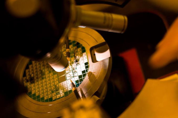
Is that like a 5-6" wafer in the image?MananDedhia - Friday, September 28, 2018 - link
Did I miss something here? To my understanding, all the RF stuff was built at the Vermont, ex-IBM fab and that has not changed - that fab is still running beyond capacity. The East Fishkill fab is used for advanced R&D on 22nm and 14nm tech nodes, but it is not cut out for production volumes. Fab 1 in Dresden will run the 22FDX node and that is solidified - and also that the 12FDX coming in later will be run in Fab 8 in Saratoga Springs NY. Can someone double check this information?P.S. : I used to work at GF Fab 8 3 years ago and this is based on my best last understanding.