ARM’s Mali Midgard Architecture Explored
by Ryan Smith on July 3, 2014 11:00 AM ESTA Brief History of Mali
ARM as a CPU designer of course needs no introduction. The vast majority of the world’s smartphones and tablets are powered either by an ARM designed CPU or a CPU based on ARM’s instruction sets. In the world of SoC CPUs, ARM is without a doubt the 800lb gorilla.
However in the world of SoC GPUs, while ARM is a major competitor they are just one of several. In fact from a technology perspective they’re among the newest, having roots that go back over a decade but still not as far as the rest of the major competitors. This is something of a point of pride for ARM’s GPU team, and as we’ll see, results in a GPU design that’s not quite like anything else we’ve seen so far.
Like all good GPU stories, the earliest history of ARM’s GPU division goes back to the late 1990s, where what would become ARM’s GPU division was first created. Originally a research project by Norwegian University of Science and Technology, the core Mali group was spun off to form Falanx Microsystems in 2001. At first Falanx was attempting to break into the PC video card market, a risky venture in the post-3dfx era that saw several other PC GPU manufacturers get shaken out – S3, Rendition, Revolution, and Imagination among them – and ultimately a venture that crashed and burnt as Falanx was unable to raise funding.
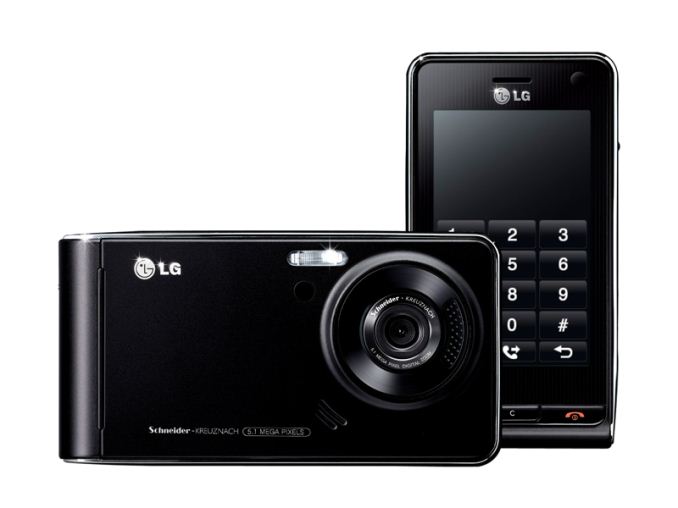
During a period of development of which they call their “scrappy phase,” due to their limited resources Falanx pivoted from designing PC GPUs to designing SoC-class GPUs and licensing those designs to SoC integrators, a much easier field to get in to. From this change in direction came the first Mali GPUs, and ultimately Falanx’s first customers. Among these were Zoran, who used the Mali-55 for their Approach 5C SoC, which in turn ended up in a couple of notable products including LG’s Viewty. But with that said, Falanx never saw great success on their own, never landing the “big fish” that they were hoping for.

LG's Viewty, One of Mali's First Wins
Ultimately as the SoC industry began to heat up from growing cell phone sales, ARM purchased Falanx in 2006. This gave ARM a capable (if previously underutilized) GPU division to create GPUs to go along with their growing CPU business. And from a business perspective the two companies were a solid match for each other as Falanx was already in the business of licensing GPUs, so for Falanx this was largely a continuation of status quo. Though for what was becoming ARM’s GPU division this was just as much of net win as it was for ARM, since it gave the Mali team access to ARM’s engineering resources and validation, capabilities that were harder to come by as a struggling 3rd party GPU designer.
Now as a part of ARM, the Mali team released their first OpenGL ES 2.0 design in 2007, the Mali-200. Mali-200 and its immediate successors Mali-300, Mali-400, and Mali-450, were based on the team’s Utgard architecture. Utgard was a non-unified GPU (discrete pixel and vertex shaders) designed for SoC-class graphics, and over the years received various upgrades to improve performance and scalability, especially on Mali-400 where Mali products first introduced the ability to use multiple cores.
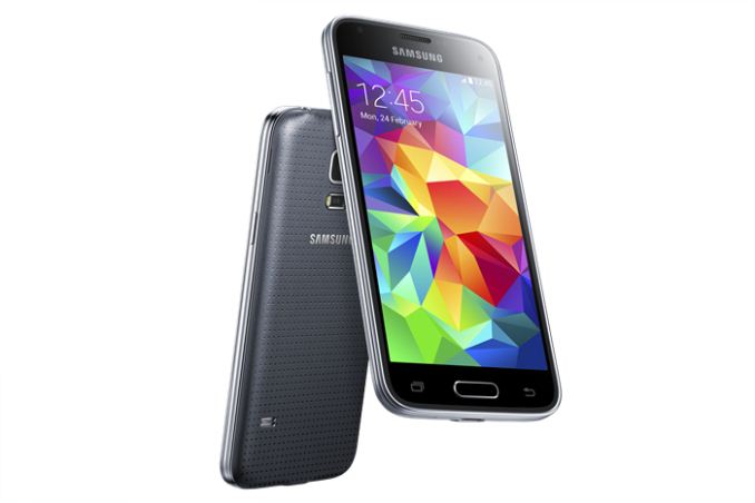
Even to this day Utgard is arguably the Mali team’s most successful GPU architecture, based in large part on the architecture’s no-frills ES 2.0 design and resulting low die space requirements. Along with driving high-end SoCs of the era, including those that have powered devices such as the Samsung Galaxy S II, Utgard remains a popular mid-range GPU to this day, with Mali-450 securing a spot just this week in Samsung’s forthcoming Galaxy S5 Mini.

Mali-450 Lives On In Samsung's Galaxy S5 Mini
Now with a team of nearly 500 people and having shipped 400 million Mali GPUs in 2013 (or as close to “shipping” as an IP licenser can get), the Mali team’s latest architecture and the subject of today’s article is Midgard. Midgard ships as the basis of ARM’s Mali-T600 and Mali-T700 family GPUs, and while it was initially introduced as a high-end architecture, it will be making a transition to cover both the high-end and mid-range through the recent introduction of more space/power/cost optimized designs. After initially replacing Utgard at the high-end last year, this year will see Utgard finally replaced in the mid-range market.


66 Comments
View All Comments
LemmingOverlord - Thursday, July 3, 2014 - link
Quick suggestion: considering Adreno is one of the most widespread GPU architectures for mobile, could you edit the table in the last page to include Adreno 3xx/4xx GPUs?Thanks!
Anand Lal Shimpi - Tuesday, July 8, 2014 - link
Unfortunately Qualcomm refuses to disclose much detail about their GPU architectures. I completely disagree with their position and have worked on Qualcomm for years to get them to open up but at this point it's a meaningless effort.da_asmodai - Thursday, July 3, 2014 - link
How about adding the Qualcomms Adreno 420 to the comparison.Anand Lal Shimpi - Thursday, July 3, 2014 - link
I wish we could - Qualcomm refuses to disclose any deeper architectural details about any modern Adreno GPU architectures.Krysto - Thursday, July 3, 2014 - link
Their loss. Plus, neither Adreno 420 nor their upcoming CPU's look that interesting or competitive anyway. Adreno 420 should still give only about HALF the performance of Tegra K1's GPU.ChefJeff789 - Thursday, July 3, 2014 - link
Really? That's disappointing... I'm really looking forward to a time when ARM, nVidia, and AMD all compete on an architectural level in their GPUs, if it ever comes. The one-horse race with Intel in the desktop CPU space has been pretty lackluster for the past few years, in terms of performance increases. nVidia's Maxwell architecture seems pretty amazing in terms of efficiency, and I'm not yet convinced AMD will be able to compete. They have yet to impress with their APU and mobile processor efficiencies.frostyfiredude - Thursday, July 3, 2014 - link
Important to note that NVidia's TK1 will be achieving that double GFLOPS performance of the Adreno 420 at a clock speed of around 950Mhz. At that performance level the TDP is listed at <10W, so it's not exactly comparable to the S805 and Adreno 420 which target a TDP half as high. What I can see happening is the TK1 being able to stretch it's legs and thus being superior in large tablets but being too thermally crippled in phones and small tablets to reach those levels. Based on the previews I found, Adreno is more efficient in it's shader resource usage, closing that further.lmcd - Thursday, July 3, 2014 - link
That's actually pretty bad math there -- if the TK1 achieves double perf at double power, it should achieve the same perf at 1/4 power (well, not quite since it isn't as simple as the basic E&M I learned, but yeah).And by your logic still, why would the K1 not fit in phones and tablets even as the 420 manages?
tuxRoller - Friday, July 4, 2014 - link
Power is linear to f, but squares with V. I don't know that we can say that at half the f you can halve the V. Actually, that's almost certainly not the case, as it's not the case with any common processor tmk.tuxRoller - Thursday, July 3, 2014 - link
The adreno 420 provides around 220gflops. The 430 well then be over 300gflops. These are not counting changes in clock speed that could raise our lower performance.