Intel 3rd Gen Xeon Scalable (Ice Lake SP) Review: Generationally Big, Competitively Small
by Andrei Frumusanu on April 6, 2021 11:00 AM EST- Posted in
- Servers
- CPUs
- Intel
- Xeon
- Enterprise
- Xeon Scalable
- Ice Lake-SP
Conclusion & End Remarks
Today’s launch of the new 3rd gen Xeon Scalable processors is a major step forward for Intel and the company’s roadmap. Ice Lake SP had been baking in the oven for a very long time: originally planned for a 2020 release, Intel had only started production recently this January, so finally seeing the chips in silicon and in hand has been a relief.
Generationally Impressive
Technically, Ice Lake SP is an impressive and major generation leap for Intel’s enterprise line-up. Manufactured on a new 10nm process, node, employing a new core microarchitecture, faster memory with more memory channels, PCIe 4.0, new accelerator capabilities and VNNI instructions, security improvements – these are all just the tip of the iceberg that Ice Lake SP brings to the table.
In terms of generational performance uplifts, we saw some major progress today with the new Xeon 8380. With 40 cores at a higher TDP of 270W, the new flagship chip is a veritable beast with large increases in performance in almost all workloads. Major architectural improvements such as the new memory bandwidth optimisations are amongst what I found to be most impressive for the new parts, showcasing that Intel still has a few tricks up its sleeve in terms of design.
This being the first super-large 10nm chip design from Intel, the question of how efficiency would end up was a big question to the whole puzzle to the new generation line-up. On the Xeon 8380, a 40-core part at 270W, we saw a +18% increase in performance / W compared to the 28-core 205W Xeon 8280. This grew to a +36% perf/W advantage when limiting the ICX part to 205 as well. On the other hand, our mid-stack Xeon 6330 sample showed very little advantages to the Xeon 8280, even both are 28-core 205W designs. Due to the mix of good and bad results here, it seems we’ll have to delay a definitive verdict on the process node improvements to the future until we can get more SKUs, as the current variations are quite large.
Per-core performance, as well as single-thread performance of the new parts don’t quite achieve what I imagine Intel would have hoped through just the IPC gains of the design. The IPC gains are there and they’re notable, however the new parts also lose out on frequency, meaning the actual performance doesn’t move too much, although we did see smaller increases. Interestingly enough, this is roughly the same conclusion we came to when we tested Intel's Ice Lake notebook platform back in August 2019.
The Competitive Hurdle Still Stands
As impressive as the new Xeon 8380 is from a generational and technical stand-point, what really matters at the end of the day is how it fares up to the competition. I’ll be blunt here; nobody really expected the new ICL-SP parts to beat AMD or the new Arm competition – and it didn’t. The competitive gap had been so gigantic, with silly scenarios such as where competing 1-socket systems would outperform Intel’s 2-socket solutions. Ice Lake SP gets rid of those more embarrassing situations, and narrows the performance gap significantly, however the gap still remains, and is still undeniable.
We’ve only had access limited to the flagship Xeon 8380 and the mid-stack Xeon 6330 for the review today, however in a competitive landscape, both those chips lose out in both absolute performance as well as price/performance compared to AMD’s line-up.
Intel had been pushing very hard the software optimisation side of things, trying to differentiate themselves as well as novel technologies such as PMem (Optane DC persistent memory, essentially Optane memory modules), which unfortunately didn’t have enough time to cover for this piece. Indeed, we saw a larger focus on “whole system solutions” which take advantage of Intel’s broader product portfolio strengths in the enterprise market. The push for the new accelerator technologies means Intel needs to be working closely with partners and optimising public codebases to take advantage of these non-standard solutions, which might be a hurdle for deployments such as cloud services where interoperability might be important. While the theoretical gains can be large, anyone rolling a custom local software stack might see a limited benefit however, unless they are already experts with Intel's accelerator portfolio.
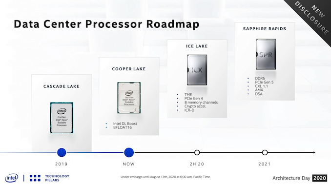
There’s also the looming Intel roadmap. While we are exulted to finally see Ice lake SP reach the market, Intel is promising the upcoming Sapphire Rapids chips for later this year, on a new platform with DDR5 and PCIe 5. Intel is set to have Ice Lake Xeon and Sapphire Rapids Xeon in the market concurrently, with the idea to manage both, especially for customers that apply the leading edge hardware as soon as it is available. It will be interesting to see the scale of the roll out of Ice Lake with this in mind.
At the end of the day, Ice Lake SP is a success. Performance is up, and performance per watt is up. I'm sure if we were able to test Intel's acceleration enhancements more thoroughly, we would be able to corroborate some of the results and hype that Intel wants to generate around its product. But even as a success, it’s not a traditional competitive success. The generational improvements are there and they are large, and as long as Intel is the market share leader, this should translate into upgraded systems and deployments throughout the enterprise industry. Intel is still in a tough competitive situation overall with the high quality the rest of the market is enabling.


169 Comments
View All Comments
deil - Tuesday, April 6, 2021 - link
that's a lot of upgrade for intelGomez Addams - Tuesday, April 6, 2021 - link
That is a curious-looking wafer. I thought it was fake at first but then I noticed the alignment notch. Actually, I'm still not convinced it's real because I have seen lots and lots of wafers in various stages of production and I have never seen one where partial chips go all the way out to the edges. It's a waste of time to deal with those in the steppers so no one does that.JCB994 - Tuesday, April 6, 2021 - link
Periphery defects? I used to deal with those...buildup of material that would breakdown during wet processing and stream particles all over the wafer. Running partials as far out as possible helped. Nowadays...do they still use big wet benches? I have been out awhile...Gomez Addams - Tuesday, April 6, 2021 - link
Yes, they do. That's one of the systems I spent lots of time working on. Those don't look defects to me. They are just a continuation of the chip pattern.FullmetalTitan - Saturday, April 24, 2021 - link
Still the most chemical efficient tools for some etch processes. It is odd to see die prints out to the edge all around, usually at least the 'corners' are inked out/not patterned by the time it hits copper layers because printing features out that far can increase the chances of film delamination, which just leads to more defectivity. I suppose on DUV tools the extra few seconds to run those shots isn't THAT bad on non-immersion layers, but it adds up over timeArsenica - Tuesday, April 6, 2021 - link
It isn´t real if it doesn´t have DrIan bite marks./jk
ilt24 - Tuesday, April 6, 2021 - link
@Gomez AddamsI spent my entire career working in the semiconductor industry, although in IT, and I have seen many wafers from 4" to 12" and printing partial die off the edge of the wafer is quite common.
check out the pictures in these article:
https://www.anandtech.com/show/15380/i-ran-off-wit...
https://www.anandtech.com/show/9723/amd-to-spinoff...
Kamen Rider Blade - Tuesday, April 6, 2021 - link
So when are we going to hit 450 mm / 18" waffers?Are we ever going to get Hexagonal Die's to maximize possible Yields?
http://www.semiconductor-today.com/news_items/2020...
https://semiaccurate.com/2015/05/18/disco-makes-he...
They can already do that for simple LED's, but trying to bring Hexagonal IC Dies into existence is going to be exciting because there is a theoretical 62.5% increase in Manufactured Dies for a given Waffer Diameter and using Hexagonal IC Dies of a similar/identical area.
ilt24 - Tuesday, April 6, 2021 - link
@Kamen Rider Blade - "So when are we going to hit 450 mm / 18" waffers?"It seems the desire to move to EUV distracted TSMC, Samsung and Intel who are probably the only companies that were really interested in 450mm.
saratoga4 - Tuesday, April 6, 2021 - link
>So when are we going to hit 450 mm / 18" waffers?For logic, never since there is little to no advantage to larger wafers. Possibly NAND might use it, but we'll see if its even worth it there.
>Are we ever going to get Hexagonal Die's to maximize possible Yields?
Probably not for logic. With reticle sizes getting smaller in the coming nodes, it makes even less sense going forward then it did in the past, and it didn't make much sense then to begin with.