Original Link: https://www.anandtech.com/show/3834/intels-silicon-photonics-50g-silicon-photonics-link
Intel's 50Gbps Silicon Photonics Link: The Future of Interfaces
by Brian Klug on July 30, 2010 6:49 AM EST- Posted in
- Intel
- Photonics
- Laser
- Trade Shows
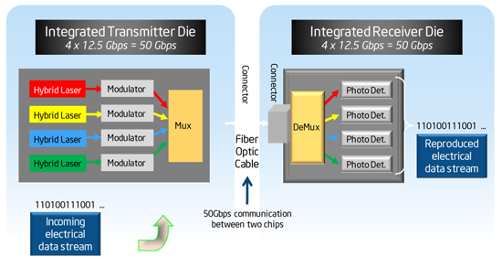
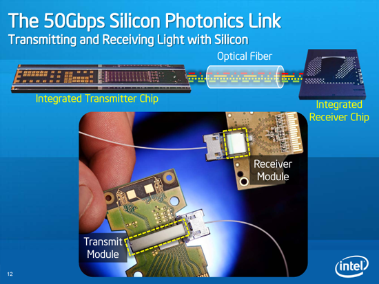
On Tuesday, Intel demonstrated the world’s first practical data connection using silicon photonics - a 50 gigabit per second optical data connection built around an electrically pumped hybrid silicon laser. They achieved the 50 gigabit/s data rate by multiplexing 4 12.5 gigabit/s wavelengths into one fiber - wavelength division multiplexing. Intel dubbed its demo the “50G Silicon Photonics Link.”
Fiber optic data transmission isn’t anything new - it’s the core of what makes the internet as we know it today possible. What makes Intel’s demonstration unique is that they’ve fabricated the laser primarily out of a low-cost, mass-produceable, highly understood material - silicon.
For years, chip designers and optical scientists alike have dreamt about the possibilities of merging traditional microelectronics and photonics. Superficially, one would expect it to be easy - after all, both fundamentally deal with electromagnetic waves, just at different frequencies (MHz and GHz for microelectronics, THz for optics).
On one side, microelectronics deals with integrated circuits and components such as transistors, copper wires, and the massively understood and employed CMOS manufacturing process. It’s the backbone of microprocessors, and at the core of conventional computing today. Conversely, photonics employs - true to its name - photons, the basic unit of light. Silicon photonics is the use of optical systems that use silicon as the primary optical medium, instead of other more expensive optical materials. Eventually, photonics has the potential to supplant microelectronics with optical analogues of traditional electrical components - but that’s decades away.
Until recently, successfully integrating the two was a complex balance of manufacturing and leveraging photonics only when it was feasible. Material constraints have made photonics effective primarily as a long haul means of getting data from point to point. To a larger extent, this has made sense because copper traces on motherboards have been fast enough, but we’re getting closer and closer to the limit.
Why use light instead of copper?
High speed PCB design is already a science in and of itself. Timing requirements dictate equal path lengths for a growing number traces between components, resulting in the ever familiar squiggly designs on desktop motherboards. Higher frequencies of course also require considerations about wave propagation through the medium - just like a transmission line. At 1 GHz, for example, one wavelength is about 0.14 meters for copper traces on FR-4, one of the most common PCB materials.
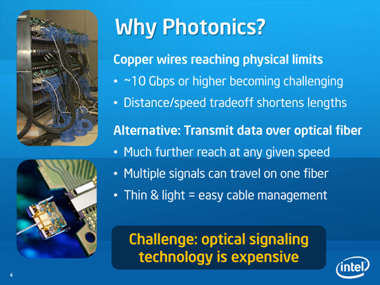
There’s also propagation delay - for wires, commonly given as 1 ns for every 6 inches of length, though different media have different wave propagation speeds due to the dielectric of the medium. I could go on about the challenges of very high frequency circuit design - which I’m not an expert in by any stretch of the mind.
The end takeaway is that traditional microelectronic designs are becoming physically constrained in size with higher and higher frequencies. You physically need to have the CPU close to the memory controller, northbridge, and other components for it to work at frequencies people expect. Move it relatively far (one wavelength) away, and the design challenges start to stretch microelectronics to its limit. Ultimately, designs sacrifice speed for distance, or vice versa.
The advantages of using optical interconnects instead of traditional copper traces are numerous. Using light instead of copper promises vastly higher bandwidth, reduced latency, resistance to electromagnetic interference, and potentially even power savings.
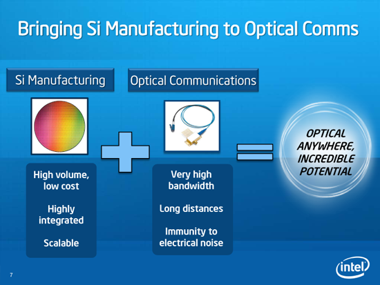
All of these reasons make using optical, silicon waveguides instead of copper traces an obvious choice. Instead of using numerous copper traces to connect the CPU to the northbridge, for example, one could envision using a single optical fiber. Or having many CPUs on one massive board connect to a chipset located even meters of path distance away. Or even have one room full of just CPUs and another room full of memory.
What Intel demonstrated on Tuesday is a working example of just that - an optical interconnect fabricated using the current traditional CMOS process, for connecting conventional electronics. Effectively an optical bus on silicon.
What’s different about Intel’s demonstration is that the lasers themselves are hybrid silicon.
It's all about Silicon
I mentioned material constraints before - without getting into too much detail, let’s talk about what makes a laser work. For every laser, you need a few things: gain medium (which should spontaneously emit photons in the presence of other photons, effectively adding optical gain), an optical resonator or feedback (in its simplest form, a cavity with mirrors at both ends), and some way of pumping (providing energy to, either electrically, optically, or whatever works for the material) the gain medium.
The problem with silicon has been that it traditionally hasn’t lent itself to creating light very well at all - it has what’s called an indirect bandgap. When electrons fall from one energy state to the other, instead of the material emitting a photon (which is what happens in a direct bandgap material), it emits primarily phonons (lattice vibrations - and through a ton of hand waving and thermodynamic processes, heat), and very few photons. In order for a material to emit large quantities photons when electrically pumped, it should have a direct bandgap.
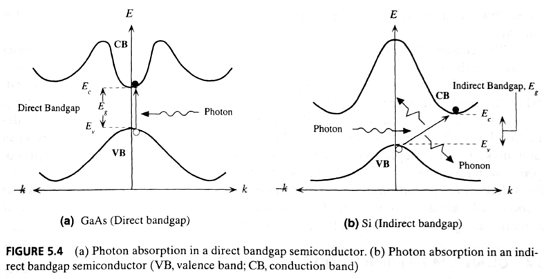
Indirect vs Direct bandgap - from Optoelectronics and Photonics: Principles and Practices by S. O. Kasap
The result for the longest time was that making a silicon laser seemed fundamentally impractical - how can something which doesn’t want to emit light be a good gain material at all?
Silicon has advantages, however. For example, silicon oxide makes an almost ideal cladding material (surrounding normal silicon). Think - fiber optic cable, but as traces embedded in your motherboard, all manufactured using traditional CMOS processes available now.
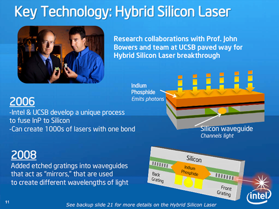
What’s new about Intel’s design - by John Bowers’ group at UCSB and a number of other researchers - is that the laser is hybrid silicon. Other previous designs have used other gain media with direct bandgaps more suitable for spontaneous emission, but with other bigger design challenges. One problem with these other materials that the crystal lattice may be too different from the silicon substrate underneath it - the result is what’s called lattice mismatch and it results in undesired optoelectronic properties. To some extent, lattice mismatch can be mitigated with an epitaxial (imagine an intermediary layer between the two mismatched material). Another problem is that thermal expansion of the materials (silicon, and whatever other material is being used for the laser) is often different as well, making it hard to physically keep things together and creating a host of other challenges. There’s also the issue of aligning the system. Previous designs have worked, at the expense of being more difficult to fabricate, and thus more expensive.

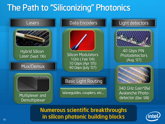
Intel’s design uses indium phosphide (InP) and aluminum gallium indium arsenide (AlGaInAs) layers, all of which can be deposited at wafer scale. The result is that there’s no discrete laser assembly or alignment. Wavelength selection and feedback are done with a distributed feedback bragg grating, which is relatively conventional. The combination of materials and manufacturing processes in this design by Intel yields itself to mass production without caveats. The end result is a hybrid silicon laser that's relatively easy to manufacture in large quantities using traditional processes.
As for the detector - bias a similar stack of components the other way, and you’re done.
Combined with Intel’s work on photonic integrated circuits on silicon for the modulator, waveguide, multiplexer and demultiplexer (for WDM), and you can see how the building blocks necessary for building optical interconnects came together.
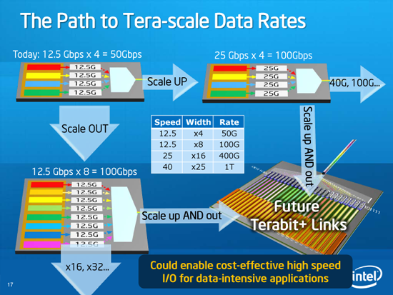
Scaling up (bitrate) and out (WDM)
Intel demonstrated an effective speed of 12.5 gigabits/s per wavelength. Using wavelength division multiplexing (WDM), one can increase the number of wavelengths (or channels) in the fiber, effectively adding more bandwidth. Intel calls this 'scaling out.' This is what’s done in virtually every long haul fiber optic telecommunications network. Even though each wavelength in conventional teleco systems might only be 10 or 20 gigabits/s, the fiber itself can carry many wavelengths, resulting in much higher aggregate bandwidth for a single fiber.